- 您现在的位置:买卖IC网 > Sheet目录1991 > CS5528-ASZR (Cirrus Logic Inc)IC ADC 24BIT 8CH 24-SSOP
CS5521/22/23/24/28
DS317F8
45
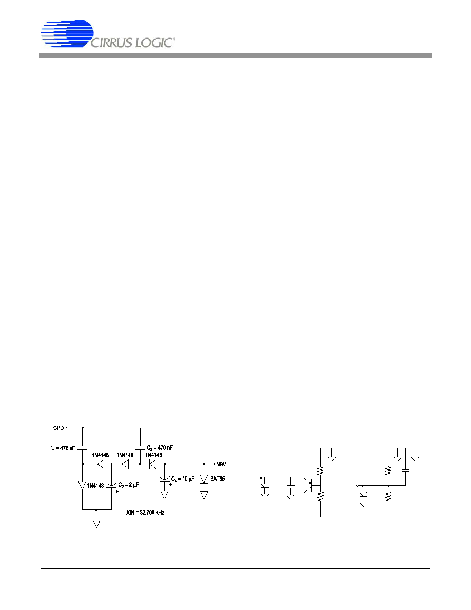
1.8.1 Charge Pump Drive Circuits
The CPD (Charge Pump Drive) pin of the converter
can be used with external components (shown in
Figure 21) to develop an appropriate negative bias
voltage for the NBV pin. When CPD is used to gen-
erate the NBV, the NBV voltage is regulated with
an internal regulator loop referenced to VA+.
Therefore, any change on VA+ results in a propor-
tional change on NBV. With VA+ = 5 V, NBV’s
regulation is set proportional to VA+ at approxi-
mately -2.1 V.
Figure 24 illustrates a charge pump circuit when
the converters are powered from a +3.0 V digital
supply. Alternatively, the negative bias supply can
be generated from a negative supply voltage or a
resistive divider as illustrated in Figure 25.
For ground-based signals with the instrumentation
amplifier engaged (when in the 25 mV, 55 mV, or
100 mV ranges), the voltage on the NBV pin
should at no time be less negative than -1.8 V or
more negative than -2.5 V. To prevent excessive
voltage stress to the chip when the instrumentation
amplifier isn’t engaged (when in the 1 V, 2.5 V, or
5 V ranges) the NBV voltage should not be more
negative than -2.5 V.
The components in Figure 21 are the preferred
components for the CPD filter. However, smaller
capacitors can be used with acceptable results. The
10
μF ensures very low ripple on NBV. Intrinsic
safety requirements prohibit the use of electrolytic
capacitors. In this case, four 0.47
μF ceramic ca-
pacitors in parallel can be used.
Note: The charge pump is designed to nominally provide
400
μA of current for the instrumentation amplifier
when
a
0.033
μF pumping capacitor is used
(XIN = 32.768 kHz). When a larger pumping capaci-
tor is used, the charge pump can source more current
to power external loads. Refer to Applications Note
152 “Using the CS5521/23, CS5522/24/28, and
CS5525/26 Charge Pump Drive for External Loads”
for more details on using the charge pump with exter-
nal loads.
1.9 Digital Gain Scaling
The CS5521/22/23/24 and CS5528 all feature a
gain register capable of being scaled from 0.6 to 4-
2-22 in decimal. The specified ranges of the con-
verter are defined with a voltage reference of 2.5 V
and the gain register set at approximately 1.0. The
gain register can be manipulated to scale the input
for ranges other than those specified. For example,
when using a 2.5 V voltage reference, and the
25 mV input range setting, the gain register can be
changed from 1.000 to 2.000 (shift the entire regis-
ter contents to the left one position) to achieve an
input span of 12.5 mV. Under this condition the
full span of the converter codes will appear across
a 12.5 mV span. The amount of noise in the con-
Figure 24. Charge Pump Drive Circuit for VD+ = 3 V
-5 V
NBV
30 .1 K
Ω
34 .8 K
Ω
2N 50 87
or s im ila r
-5V
2.1 K
Ω
2.0K
Ω
NBV
+
10
μF
10
μF
+
BAT85
Figure 25. Alternate NBV Circuits
发布紧急采购,3分钟左右您将得到回复。
相关PDF资料
CS5529-ASZR
IC ADC 16BIT W/6BIT LATCH 20SSOP
CS5530-ISZR
IC ADC 24BIT 1CH W/LNA 20-SSOP
CS5534-ASZR
IC ADC 24BIT 4CH W/LNA 24-SSOP
CS5534-BSZR
IC ADC 24BIT 4CH W/LNA 24SSOP
CS5550-ISZR
IC ADC 2CH LOW-COST 24-SSOP
CS5565-ISZ
IC ADC DELTA-SIGMA 24BIT 24-SSOP
CY28317PVXC-2
IC CLK FTG VIA PL/E133T 48SSOP
CY28323OXC
IC CLOCK BROOKDALE GPENT4 48SSOP
相关代理商/技术参数
CS5529
制造商:CIRRUS 制造商全称:Cirrus Logic 功能描述:16 BIT PROGRAMMABLE ADC WITH 6 BIT LATCH
CS5529_05
制造商:CIRRUS 制造商全称:Cirrus Logic 功能描述:16-bit, Programmable ΔΣ ADC with 6-bit Latch
CS5529-AP
功能描述:模数转换器 - ADC Prgrmmbl Delta Sigma ADC w/6-Bit Lat-Ch RoHS:否 制造商:Texas Instruments 通道数量:2 结构:Sigma-Delta 转换速率:125 SPs to 8 KSPs 分辨率:24 bit 输入类型:Differential 信噪比:107 dB 接口类型:SPI 工作电源电压:1.7 V to 3.6 V, 2.7 V to 5.25 V 最大工作温度:+ 85 C 安装风格:SMD/SMT 封装 / 箱体:VQFN-32
CS5529AS
制造商:CIRRUS 功能描述:New
CS5529-AS
功能描述:模数转换器 - ADC Prgrmmbl Delta Sigma ADC w/6-Bit Lat-Ch RoHS:否 制造商:Texas Instruments 通道数量:2 结构:Sigma-Delta 转换速率:125 SPs to 8 KSPs 分辨率:24 bit 输入类型:Differential 信噪比:107 dB 接口类型:SPI 工作电源电压:1.7 V to 3.6 V, 2.7 V to 5.25 V 最大工作温度:+ 85 C 安装风格:SMD/SMT 封装 / 箱体:VQFN-32
CS5529-ASZ
功能描述:模数转换器 - ADC Prgrmmbl Delta Sigma ADC w/6-Bit Lat-Ch RoHS:否 制造商:Texas Instruments 通道数量:2 结构:Sigma-Delta 转换速率:125 SPs to 8 KSPs 分辨率:24 bit 输入类型:Differential 信噪比:107 dB 接口类型:SPI 工作电源电压:1.7 V to 3.6 V, 2.7 V to 5.25 V 最大工作温度:+ 85 C 安装风格:SMD/SMT 封装 / 箱体:VQFN-32
CS5529-ASZR
功能描述:模数转换器 - ADC IC Prgrmbl Dlt Sigma ADC w/6-Bit Latch RoHS:否 制造商:Texas Instruments 通道数量:2 结构:Sigma-Delta 转换速率:125 SPs to 8 KSPs 分辨率:24 bit 输入类型:Differential 信噪比:107 dB 接口类型:SPI 工作电源电压:1.7 V to 3.6 V, 2.7 V to 5.25 V 最大工作温度:+ 85 C 安装风格:SMD/SMT 封装 / 箱体:VQFN-32
CS5530
制造商:Texas Instruments 功能描述: